Maskless lithography

Several attempts have been made to produce maskless lithography via an
liquid crystal display. This has led to two diploma work at
Linköping
University and Umeå University.
first experiment
The first experiments were made with a disassembled pocket calculator
displays to verify the method to expose pattern directly on
photoresist. In this case a simple contact copying procedure was
performed. A pattern in the form of digital signs from the
display were copied directly to the photoresist. It worked fine to
prove the method.

This is an image of the result from the contact copying experiment,
13:th November 2001 An ordinary mercury lamp was used and
the display was pressed directly on the photoresist coated
glass.
Second experiment
The second attempt were done with an transmittive LC display from
Kopin. It was a small display with resolution of ca 290 X 218 pixels. The
pixel pitch were circa 15um. This display was placed in the Gloria 2x
reduction UV projector. Due to very low etendue, exposure times
of 2-3 minutes were needed. However very fine patterns were made.
The Gloria projector had a Rodenstock Apo rodagon N with 2x
reduction and 50mm focus. It was the best available optics for a low
cost. It had quite good MTF and large aperture. However designed for
the whole visible spectrum and in this case only 405nm wavelength were
used. It was not possible to do any simulation becouse of the
unknown lens curvatures. Some data of NA is however avalible for
the whole visible spectra..
MTF of Apo rodagon N 50mm.
lens data page 1
lens data page 2
This image shows the finest lines in
the bottom of the picture, wich are only one pixel wide. Due to
the reduction optics the line with is appr 5um wide.
Here is a close up of the kopin display. Model RS170. Electronic datasheet of the RS170 and a short description of the pin configurations.
The Kopin display was mounted on an aluminum frame wich hold the drive
electronics also. In this way the whole assembly could easily be
pushed into the gloria UV projector instead of the reticle.
image of the whole display.
Third experiment
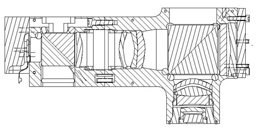
A more complex solution were needed if high numerical aperure and MTF
should be reached. This was necesery if short exposure times and high
resolution is a goal. The best choice were a catadioptric design
wich incorporated a mirror and lenses. Polarised light were used to be
able to link off the light without obscuration in the light path.
The light was circulary polariced in a quarter wave plate to turn
the polarisation angle 90 degrees in the second path, and the light
could be linked down in a cube beamsplitter. This also enabled
the use of the polarisation beam splitter as an aperture for a focusing
laser. Many other issues were also solved in this design. It could be
made very compact, high etendue, even a option of a CCD camera, mounted
over one polarisation beam splitter and take real time image on the
exposure area from a dark field microscope mounted on top.This function
was critical if mask alignment could be used in multi layer devices.
The report from VTT Electronics. (pdf)
VTT managed to achive very good MTF for the lithographic lens. The
major goal was to be able to assemble the 14 different optical
components in just two NC machined block without post adjustment. This
made the lens very suited for massproduction.
MTF for the second lens. Take in
account that this MTF was measured without the coverglass from the Lcos
display wich cause appr. 10 percent lower MTF value than it
actually is. At 300-400 l/mm there is a slight measuring error due to
limitations in the slitwith in the measuring equipment.
The diploma reports
Autofocusering av litografisk lins med astigmatisk metod.(word)

The setup with a Nd:YAG laser for astigmatic focusing at +/-3um.
Microlithography_for_half_tone_gobos (word)
Microlithography for half tone Gobos (pdf)

An image of the prototype, still without the autofocusing and the positioning table.

This LED lamp was used for some of the exposure tests. 91 parallell GaN diodes collimated by a 50mm large condensor lens.
this research system was Developed by VTT Electronics in Finland. Some
practical tests were performed in Jönköping and later in
Norrköping at ITN. The tests were performed without proper
focusing but in theory an astigmatic focusing system could be
used, integrated in the system. Also some inventive lightsource
with GaN LED source could replace unplesant ultra high pressure
mercury discharge lamps.
This image shows an early attempt to prove the resolution of the
system. A line pattern was created via the Lcosdisplay and blue
405 nm light from an array of GaN LEDs produced this pattern. image.
The first sucessful exposure on a photoresist coated a glass
substrate. The diameter of the glass is 37.5mm. An image was
created from a computer screen. The display is not masked
yet. image.
One of the first test of a full scale rastered image. Note some
vertical lines over the image. These are from dead pixel rows
from the display. Still the image lack of uneven exposure and bad focus. image.
Chrome etching with ceriumcompound


